Design a PCB To Pass EMC As A Medical Electronic Device
By Parker Bondi
February 19, 2025
Recently I completed a challenging design project for my customer in the medical electronic equipment industry. In this article I will share the steps and tools I used to modify a design to ensure it passes the EMC requirements for products to be sold in North America and Europe. It all began with a few conversations about their working prototype. The customer’s device was a 6-layer 6in x 3in battery powered high speed digital signal processing PCB. It was clear that they were having issues passing the emission requirements and they needed help.
What are the Regulatory Requirements for Medical Electronic Devices
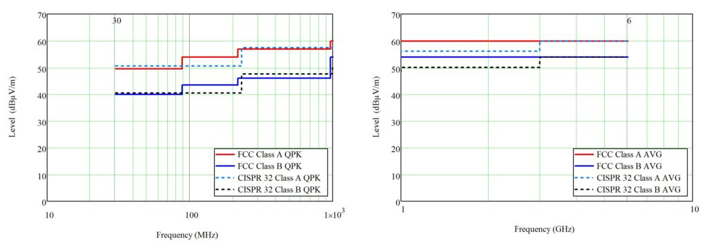
The International Electrotechnical Commission (IEC) is the standards organization that defines the regulatory requirements for medical electronic devices. IEC 6100 states that medical electronic equipment must meet the Class B Conducted and Radiated Emissions standards for multimedia equipment specified for each desired region for sale.
- The Conducted and Radiated Emissions threshold for the sale of devices in Europe is defined by the CISPR 22 European Norms (EN) 55022 (now updated to CISPR 32/EN 55032) Class B standard.
- The Conducted and Radiated Emissions threshold for the sale of the product in North America is defined by the FCC Part 15 Subpart B standard.
The “TI Review of EMI Standards” can assist designers in determining the requirements for their devices.
Here are links to Part 1 & Part 2:
Describing EMC
The methods by which noise radiate out of a PCB are well described by Wurth Elektronik’s application note: Impact of the layout, components, and filters on the EMC of modern DC/DC switching controllers. This note describes the difference between common-mode interference and differential-mode interference. It also discusses the characteristics of the current flowing through the two loops that are fundamental to the working principle of a step-down converter. Recently, Robert Feranec’s video Simple Trick to Improve EMC – Easy Filter Design for Power Supply with Thomas Eichstetter elegantly described these loops and their impact on EMC test results.
Finding The Issue
The customer was using a Power Management IC (PMIC) as well as a boost converter to provide their PCB with multiple voltage rails. The PMIC has 3 synchronized 2.2MHz fixed-frequency buck converters powering their digital electronics while the boost converter has a switching frequency of 1.2MHz and supplies the analog sensing electronics.
Common-Mode Filter Design
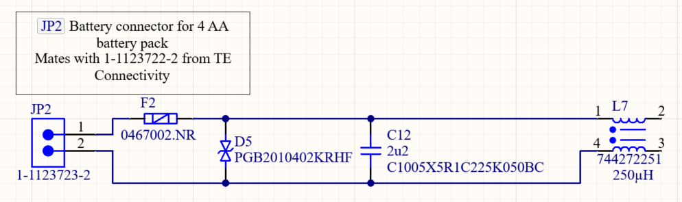
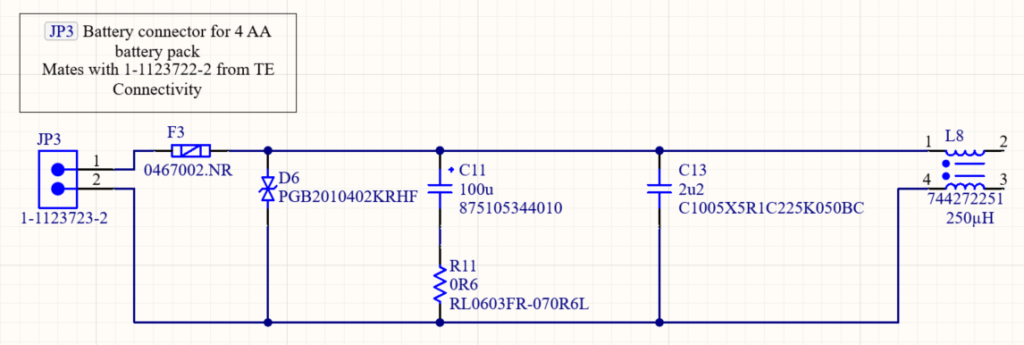
With this in mind, the investigation started at the battery connector. Here the electronics have a safety circuit followed by a common mode line filter similar to (but not the same as) the circuit below.
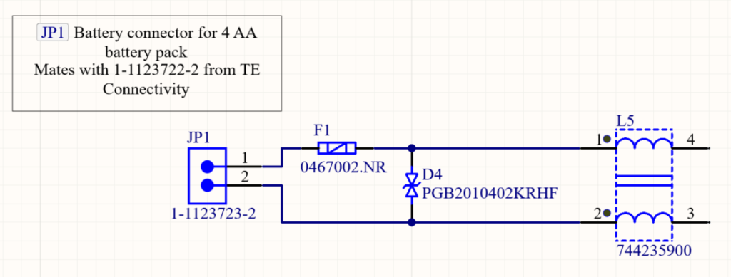
Line filters are commonly used for applications like this to suppress common mode noise from radiating out through the battery. However, Wurth Elektronik’s REDEXPERT simulation tool shows that the common-mode impedance of 744235900 below 2MHz is negligible and the differential-mode impedance below 10MHz is negligible.

This means that the switching noise will pass through this device if it is present as a common-mode or a differential-mode noise.
To solve the common-mode noise problem this design needs a common-mode line filter with a wider bandwidth. This new device will also need to maintain a margin of safety over the maximum current and voltage on this net as well as fit inside the mechanical housing. The original line filter had a maximum current rating of 2A and 60V. The mechanical housing has approximately 10mm of vertical space above the PCB.
The 744272251 from Wurth Elektronik meets these requirements and has a high common-mode impedance down to 10kHz.

Differential-Mode Filter Design
To solve the differential-mode noise problem a capacitor can be combined with this line filter to create a LC lowpass filter.
Wurth Elektronik’s Application Note: 1-Phase Line Filter Design as well as Wurth Elektronik’s Trilogy of Magnetics – Design Guide for EMI Filter Design, SMPS & RF Circuits both suggest when you are unable to test the electronics it is a good practice to design the input filter to a step-down converter with at least 40dB of attenuation at the switching frequency.
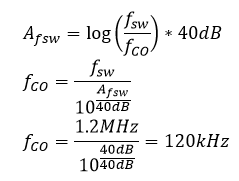
This corner frequency along with the inductance of the common-mode line filter can be used to determine the capacitance required to attenuate noises in this frequency range.
Due primarily to the imbalance of the windings within the common-mode line filter they can act as an inductor to differential-mode signals. This inductance is known as the leakage inductance and can be found in the datasheet of most devices or it can be calculated from the differential-mode impedance curve. This is well described in Application Note: 1-Phase Line Filter Design. The datasheet of the 744272251 states that the leakage inductance is 1500nH.
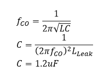
A common capacitor value in this range is 2.2uF. A voltage rating of 16V was sufficient factor of safety for 4 AA batteries. A small package size to reduce the ESL was found to be a 0402. The C1005X5R1C225K050BC from TDK met all of these requirements.
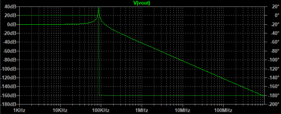
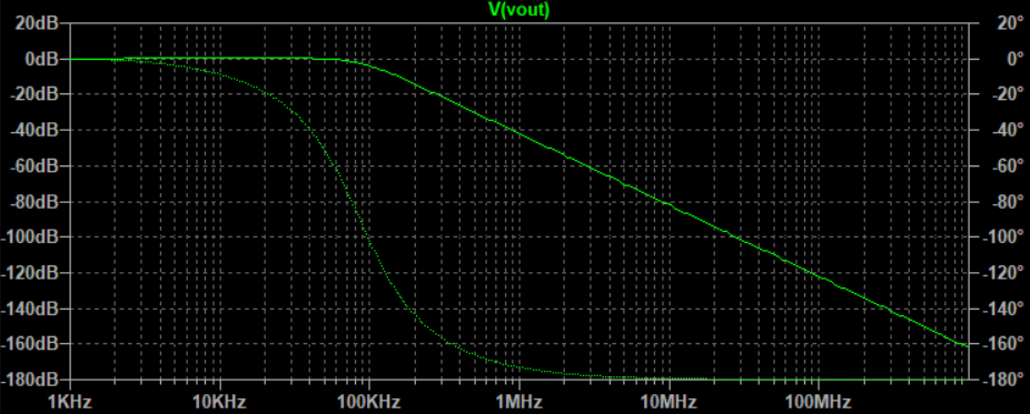
This filter shows good -45dB attenuation at 1.2MHz however it also shows a strong resonance at 87kHz. This means that signals at 87kHz could be significantly amplified. This is why the application note above highly recommend an additional parallel RC damping circuit.
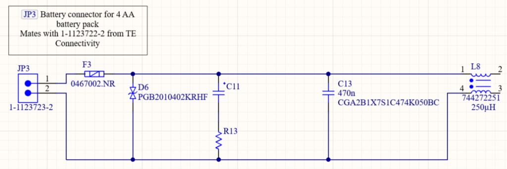
The Impact of the layout, components, and filters on the EMC of modern DC/DC switching controllers on page 5 states that a dampening factor of 0.707 in the transfer function of the circuit will provide good attenuation of the resonant frequency but not affect the corner frequency of the filter. The dampening factor can be calculated using the following equations.
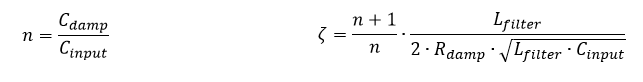
The dampening capacitor should be at least 4x the capacitance of the input capacitor however much larger capacitance with low ESR is even more optimal for this situation. Therefore, a 100uF aluminum polymer capacitor with a 16V rating and low ESR was selected which then resulted in a dampening resistor of 0.60Ohms. The 875105344010 from Wurth Elektronik was chosen due to its high capacitance and low ESR to allow the dampening resistor to dominate the series resistance of the two devices. The resistor was chosen to be the RL0603FR-070R6L from Yageo because of its small 0603 package and accuracy.
Switch-Mode-Power-Supply Decoupling Capacitors for Better Local Charge Storage
I refer to a few great resources when designing buck converters on PCBs. Wurth Elektronik’s Trilogy of Magnetics – Design Guide for EMI Filter Design, SMPS & RF Circuits describe how the issue of sharp current draws from the buck converter causes large ripple currents on the supply line when there is no local low impedance energy reservoir. Robert Feranec’s video Simple Trick to Improve EMC – Easy Filter Design for Power Supply with Thomas Eichstetter describes the two states of a buck converter using two current loops. One loop for when the buck converter is drawing power from the power supply, and the other for when the inductors magnetic field has inverted and is providing the power.
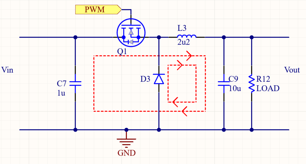
In the video they show how the inductor and output capacitor always have current flowing through them but the diode, input capacitor, and MOSFET switch from very high current draw to zero current draw. These three components experience a large negative dI/dt and these are the components that are the most critical to design correctly.
In the customers prototype the three buck converters used the 10uF, 10V, 0805 ceramic capacitor C2012X5R1A106M125AB from TDK Corporation which is no longer being manufactured. The GRM155R61A106ME11D from Murata is a better choice because it has the same capacitance and voltage rating but is in a smaller package size of 0402 thus reducing the ESR and ESL.
PCB Stackup for Better Return Paths
The boards stackup was similar to many 6-layer stackups that are notorious for poor signal return paths that is critical for high performance PCBs with modern components.
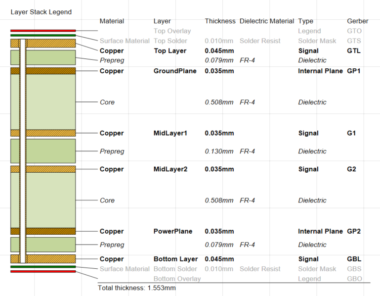
In this board the Top Layer, MidLayer1, MidLayer2, and Bottom Layer were all used to route signals to and from the components placed on the Top and Bottom of the PCB. The GroundPlane was split into 2 isolated planes, the PowerPlane was split into many different planes, and the routing layers had ground poured throughout the remainder of the open space. The design also had stitching vias connecting the majority of these copper sections of ground together.
This is a problem for the high frequency modern electronics on the circuit board. For a full understanding of this concept I would highly recommend reading Fast Circuit Boards: Energy Management by Ralph Morrison. From this understanding an 8-layer board would provide contiguous return paths however due to other changes in the design the following 10-layer stackup was chosen.
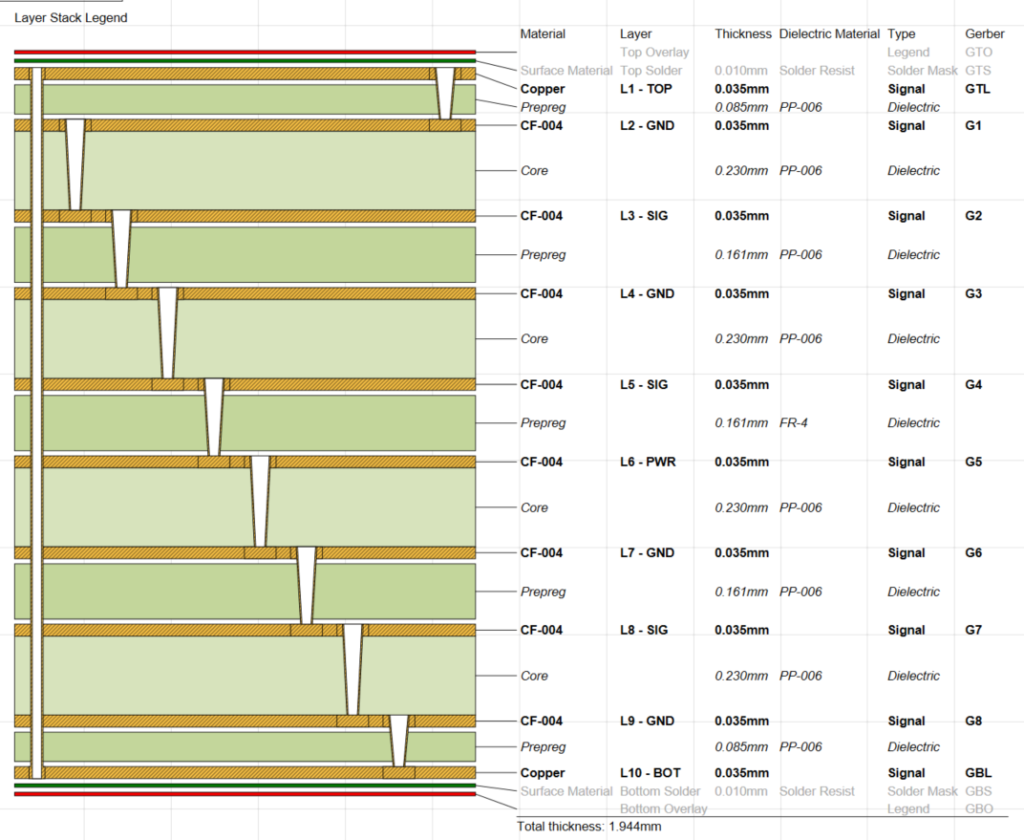
While it is possible to design a stackup with custom prepreg copper, and core thicknesses. It is much more economical to choose a predefined stackup that your manufacturer has readily available. This particular stackup was selected from PCBWay’s predefined stackups. With this design every layer has a contiguous ground plane directly above or below it providing optimal return paths.