How to Choose a PCB Stackup
By Parker Bondi
November 2, 2025
In this article I will walk the reader through the step by step procedure I use to choose and optimize the stackup for my PCBs with details on why I chose that stackup, the resources I used, and the theory behind these choices.
Partnership Announcement
This article has been written in partnership with PCBWay to highlight the aspects of their PCB Fabrication and Assembly tools and resources that I use during the first stage of my PCB Layout process.
PCBWay is my go-to manufacturer and if you are looking to design your own high quality PCBs check them out and enjoy a small discount by using my referral link!
Common Project Starting Points
In the consulting business the projects that you are introduced to start at a variety of breakpoints in the design process. Sometimes it is as early as a block diagram and sometimes it’s passing compliance testing.
This article will focus on the design process for a brand new board which has never been laid out before. However, there will be many practical applications of these steps for other projects where I have needed to redesign parts or whole boards as well, but the process for redesigning a board can take aspects from these steps.
Starting a New Design
From a big picture perspective, routing typically consists of:
- Defining a stackup
- Creating rules
- Major component placement and grouping
- Major component routing (or priority trace routing)
- Minor component placement and grouping
- Minor component routing
When starting a new design with components I have never used in the past I commit myself to routing the board twice. First a preliminary routing and second an optimized design. I have found this technique to be efficient due to its resourcefulness of the work it takes to get to this stage in the design development process.
Preliminary Design Overview
At a very high level the preliminary design is a high fidelity block diagram. I basically take the block diagram, sketches of the product, and mechanical features of the product into consideration to partially place, fanout, and route the main components of the design. Once I have placed the main components on the preliminary design I take a few key details that I need for the optimized design, backup the design file, review the details, and begin the optimized design at the stackup.
The reason for this technique is because I find it is resourceful in the fact that you are using work you have already completed to assist in the design of the fundamental aspects of the final PCB layout.
Block Diagram
Projects often begin with a block diagram, and if they don’t begin with it, they are often used to convey the product’s intent and logic. A well-structured schematic can also be similar to a block diagram. Block diagrams also have the major components. I’d like to share the block diagram of a simple project I worked on last year – a nRF52 based accelerometer project.
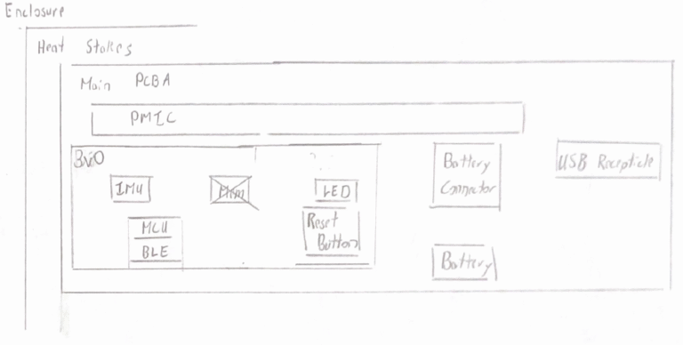
In the preliminary design I partially route the main busses in the block diagram. Whatever main ICs are included on the block diagram I pull into the PCB environment from my schematics and put them into the locations defined by the block diagram. I don’t overcomplicate this process because I know this board will be scrapped and it is a tool to assist in the definition of the final stackup and board constraints.
Reviewing and Learning from the Preliminary Design
After this preliminary routing I review the design and run through the following checklist:
- What are the mechanical requirements?
- What layer did I use ineffectively?
- What impedances do I need & where?
- Am I using my power plane effectively?
Here I am finally able to define a layer count and begin the final layout.
Final Design Process
Selecting a Stackup
The next step is to find the perfect stackup from this layer count. I find myself always referring back to PCBWay’s Standard Stackup online tool (https://www.pcbway.com/multi-layer-laminated-structure.html) to find a stackup that works for me. Currently PCBWay defines 298 stackups that designers like myself can utilize with ease because PCBWay classifies them as “standard”.
- 112 4-layer stackups
- 74 6-layer stackups
- 49 8-layer stackups
- 33 10-layer stackups
- 12 12-layer stackups
- 6 14-layer stackups
- 6 16-layer stackups
- 6 18-layer stackups
Many boards I have designed in the past have 90Ohm USB differential impedance traces or 50Ohm impedance requirements. These traces are often the narrowest width traces that I route on my PCBs. So I typically start by applying the stackup filter to PCBways website based on layer count and take the dielectric thickness and dielectric constant and put it into my saturn PCB design tool to calculate a 90 Ohm differential pair impedance on an edge coupled asymmetric stripline setup.
PCBWays standard stackups is such a great tool because all of the information I need to determine my trace dimensions is available right in front of me.
Once my Saturn PCB tool has suggested a trace width I check that against PCBWay’s manufacturing capabilities. The great thing about PCBWay’s capabilities table is that they are stratified with complexity and other related variables. For example the first section defines a trace width minimum of 0.1mm but strongly suggests to design above 0.15mm to save cost. This is their recommendation for quick-turn PCBs. Further down they describe their advanced PCB fabrication capabilities with track width stratified further against the copper thickness and process difficulty (normal, medium, high). With a medium difficulty advanced PCB and 1oz copper the track width and spacing is defined as 0.12 mm. This is the area I try to avoid.
I start by define the board stackup, define my design rules and constraints according to manufacturing limitations, and apply improvements to the component placement based on the block diagram. Finally I begin to route and that is a story for another day.
Get in touch with us
Did you know stackups could be easy sometimes? Contact us and let us help!