USB-C Routing
By Parker Bondi
October 2, 2025
USB-C’s flip-ability is one of the most user-friendly features, allowing the cable to be inserted in either orientation without hassle. However this convenience presents a unique routing challenge to maintain impedance, phase alignment, and minimize stub length. Buckle up, we’ll touch on all three of these fundamental principles and share the resources along the way!
USB-C Schematics
Making your circuit board able to accept the USB-C cable in either orientation requires the two sets of Dp and Dn differential pairs to be connected together. Dp1 must be connected to Dp2 and Dn1 must be connected to Dn2.

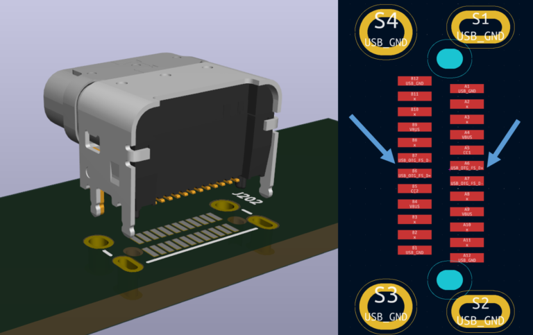
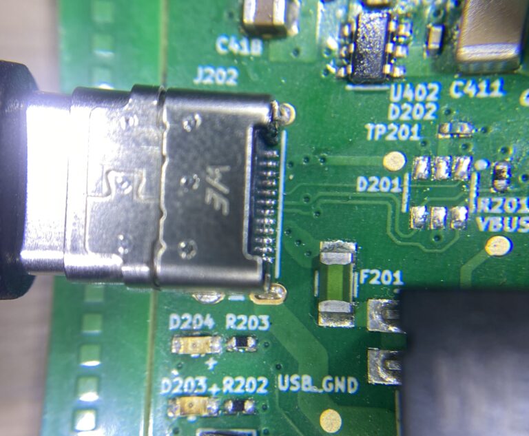
USB-C Connector Footprint
The USB-C connector has the differential signals coming out on both rows of the footprint. The pads are 0.3mm wide and 0.5mm pitch leaving only 0.2mm between them which is tight when you consider that basic fabrication abilities for low cost PCBs require trace widths >0.15mm.
Routing
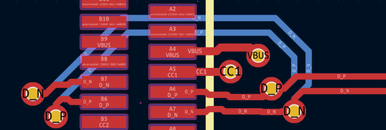
Here we have a 4 layer board with 90 Ohm differential impedance controlled stackup and routing on the top and bottom layers of the PCB. The right side is routed out simply, while the left is immediately routed down to the bottom layer and loops around the traces to correct for the flip-ability of the footprint. We’ve left space for 2 vias for VBUS and CC1 if they are necessary. Lets look into all 3 of our important principles to determine if this is acceptable for a USB 2.0 High Speed implementation of the USB protocol running at 480MBps.
Impedance
With constant track width and the ability to maintain the differential trace spacing we’re looking at impedance discontinuities due to the pads and via design. Is this a problem?
Stubs
If the plug is not flipped, signals come out of pins A6 and A7 and propagate down the traces. Those signals come across the via and part of the signal propagates down the via into the traces on the bottom layer all the way to pins B7 and B6 and back while the transmitted signal continues to propagate down the traces on the top layer. We’ve created a stub! Is it long enough to cause a problem?
If the plug is flipped the same issue arises, however the stub length is significantly shorter. Is it still a problem?
Phase
If the plug is not flipped the two stubs are different lengths. D+ stub is 8.9mm while the D- stub is 10.0mm. Is this a problem?
Reflections
Electrical energy in printed circuit boards propagates as a wave guided by the copper traces. They see only the characteristic impedance of the transmission line they are propagating along. This wave is dynamic and interacts with other waves that share the transmission line with it.
Signals see the characteristic impedance as they propagate down the transmission line. – Eric Bogatin
At every impedance discontinuity along a transmission line there is a part of the wave that transmits and a part of the wave that reflects.
The transmission coefficient is the ratio of the transmitted signal amplitude to the incident wave amplitude.
The reflection coefficient is the ratio of the reflected wave amplitude to the incident wave amplitude.
Transmission coefficient = Vtrans / Vincident
Tcoeff = 2 x Z2 / (Z2 + Z1)
Reflection coefficient = Vreflected / Vincident
Rcoeff = (Z2 – Z1) / (Z2 + Z1)
When a 0-1V signal travels down a transmission line and hits an open it reflects.
- The original signal has a direction of propagation from left to right
- The original signal has a direction of circulation that is clockwise
- The reflection coefficient is 2
- The reflected signal has a direction of propagation from right to left
- The reflected signal has a direction of circulation that is counter-clockwise
- Voltages add up
- Currents cancel
- This is why you don’t have current at an open
- The original signal has a direction of propagation from left to right
- The original signal has a direction of circulation that is clockwise
- The reflection coefficient is -1
- The reflected signal has a value of -1 and a direction of propagation from right to left
- The reflected signal has a direction of circulation that is clockwise
- Voltages cancel
- Currents add up
- This is why you don’t have voltage at an open
When is a Stub Long Enough to Cause A Problem?
The fundamental problem with impedance discontinuities are reflections. Where the incident wave arrives at the receiver with effects from the reflected waves it generated along the way.
Signals arrive at our USB-C connector and see the low impedance of the wide smt mounting pads and reflect.
Signals continue down the transmission line to the via and see the low impedance of the vias and reflect.
I like to imagine taking the cylindrical barrel of the via and unwrapping it to create a trace that is as wide as the circumference of the barrel. Going vertically through the PCB is different from horizontally and the impedance of a via is very complicated due to non-linear interactions, and some counter intuitive features.
This sounds really bad but it is not the full story of the signal traveling down the transmission line. In addition we see an impedance discontinuity when the signal goes from the wide smt pad to our traces. Likewise as the signal is traveling down the vias it sees an impedance discontinuity when it goes back into the traces. These interfaces reverse the transmission coefficient equation, which doesn’t revert our signal back to the original, but it does recoupe some of its amplitude. You could imagine that this analysis could continue further to impedance discontinuities from the corners of the traces or changes is the dielectric constant due to fiber weave pattern in the glass. The analysis could go on, but at some point we don’t care because at the end of the day the effect of these minor impedance discontinuities is to increase the rise time of the signal.
The fundamental issue with the stub architecture is reflections.
- A wave will propagate down to the end of the stub, reflect back, and interfere with the incoming signal.
With a 1/4 wavelength phase delay a 100% differential signal becomes 50% differential and 50% common! – Eric Bogatin.
Now let’s consider the design that we have where the stub begins on the right side of the USB-C connector goes down to the bottom layer to the other side of the connector and back up to the top layer. The overall stub length is:
- 1.6mm via
- 9.6mm bottom layer
- 1.6mm via
- 1.9mm top layer
- 1.1mm pad
Since this is a generic article, let’s look into a theoretical requirement based on our understanding of signals.
The bandwidth of a signal is often defined from the rise time of that signal. Typical rise times of 10% result in a bandwidth that is 5x the fundamental frequency of the signal. In other words the bandwidth includes frequencies up to the 5th harmonic (1.2GHz for USB 2.0). The period of this frequency is 1/5th of the eye diagram. This would be a good starting point to say with confidence that our receiver is able to capture the signal. Let’s assume a factor of safety such that our signal we are providing our receiver is even better than the 5th harmonic and design the eye diagram for the 7th harmonic which is 1.68GHz or 595ps.
Now that we determined the margins of our acceptable eye diagram what does this mean in terms of acceptable stub length? We have to think about whether or not the propagation time down and back from this stub is significant relative to our comfortable eye diagram requirement. Doing so results in the comparison of the 595ps requirement vs the 226ps stub and we find that this is acceptable.
Mode Conversion
The fundamental problem with poor phase alignment is mode conversion. Where differential signals are inadvertently converted into common signals.
A differential signal is the difference between the two signals.
Differential signal = Dp – Dn
A common signal is the average of the two signals.
Common signal = (Dp + Dn)/2
How much phase mismatch is too much? It depends on how good your receiver is and how much of the total transmission line budget you can allocate to your board.
With a 1/4 wavelength phase delay a 100% differential signal becomes 50% differential and 50% common! – Eric Bogatin.
When is Mode Conversion a Concern for USB 2.0 High Speed?
Start by calculating the total transmission line budget. Determine the nyquist of the signal – for USB 2.0 High Speed which operates at 480MBps that is 240MHz which has a period of 4.2ns. Following the generalizations above we will build off of the theoretical eye that we were providing the receiver and state that we would like to keep phase mismatch less than 5% of the UI (to keep our 90% eye opening). That results in a length matching requirement of 208ps or 29mm in our FR-4 board.
When the plug is flipped and the signals come out of the B6 and B7 pins the D+ and D- traces are 8.9mm and 10mm respectively resulting in a phase mismatch of 1.1mm. This is far less than the 29mm defined by this requirement so we find again that this routing is acceptable.
Get in touch with us
Are you looking to design and develop USB-C circuit boards? Contact us and let us help!